On July 14, 2026, the Ministry of Economy, Trade and Industry announced that it would provide up to 159 billion yen in subsidies to Tower Semiconductor, a major Israeli semiconductor contract manufacturer. This massive investment is a crucial step in establishing a domestic production base for next-generation communication technologies against the backdrop of rapidly increasing AI demand, thereby strengthening economic security.
- 159 billion yen subsidy and production plans in Niigata and Toyama
- The Impact of the Critical Point in the AI Era: ‘Silicon Photonics’
- Diversification of the “Israel Risk” and Japan’s Strategic Advantage
- Collaboration with NTT and Building a Regional Ecosystem
- Tower’s Dual-Track Strategy and 2028 Goals
- The semiconductor boom spreading from Hokuriku and its ripple effects on the regional economy
- Future outlook and lessons to learn from “past failures”
159 billion yen subsidy and production plans in Niigata and Toyama
On July 14, 2026, the Ministry of Economy, Trade and Industry decided to provide up to 159 billion yen in subsidies to the Japanese subsidiary of Israel’s Tower Semiconductor. This project aligns with the government’s policy of designating semiconductors as “specified critical materials” under the Economic Security Promotion Act. The total project cost is approximately 600 billion yen, and we will mass-produce cutting-edge optical communication semiconductors (silicon photonics) by utilizing existing bases in Myoko City, Niigata Prefecture and Uozu City, Toyama Prefecture. Specifically, the Niigata factory will begin operations in May 2027, and a new production base in Toyama is scheduled to be built and supply will begin within 2028. Please refer to the diagram below.
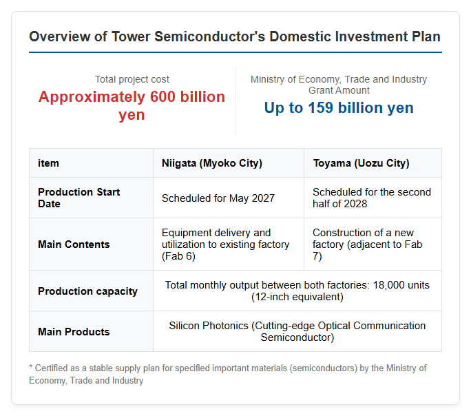
The combined production capacity of both sites is aimed at 18,000 wafers per month (equivalent to 12-inch wafers), which is expected to make it one of the world’s largest silicon photonics manufacturing bases, surpassing the company’s current U.S. base. This investment is expected to dramatically strengthen the stable supply system for advanced semiconductors within Japan.
The Impact of the Critical Point in the AI Era: ‘Silicon Photonics’
The main reason this investment is considered important is that the semiconductors being mass-produced are silicon photonics, which forms the core of “optoelectronic fusion technology.” Silicon photonics is a technology that integrates optical circuits on a silicon substrate and exchanges electrical and optical signals, simultaneously achieving communication speed and significant power consumption reductions that were difficult with conventional electronic circuits. Currently, with the explosive spread of generative AI (artificial intelligence), data centers worldwide are rapidly increasing both communication volume and power consumption, making demand for this technology indispensable. Tower boasts the world’s top market share in optical communication semiconductors, and introducing its advanced manufacturing technology to Japan carries extremely strategic significance as it will determine the competitiveness of Japan’s AI infrastructure. This technology is also essential for implementing the next-generation communication infrastructure “IOWN,” which transmits information via light rather than electricity, and is expected to become a technological breakthrough supporting the foundation of Japan’s digital society.
Overcoming geopolitical risks and strengthening resilience through domestic collaboration
Diversification of the “Israel Risk” and Japan’s Strategic Advantage
For Tower, headquartered in Israel, this large-scale investment in Japan is based on a strong management logic to diversify geopolitical risks. Since 2023, the escalating tensions in the Middle East have brought to light the impact of risks in the country where headquarters are located on business continuity, known as the so-called “Israel risk.” In such unstable circumstances, strengthening mass production bases in Japan, which has stable power and mature manufacturing infrastructure, is an extremely rational choice both for Tower and for its global customers. On the other hand, for Japan, bringing supply chains that have relied on regions with high geopolitical risks into the country offers significant economic security advantages. This investment is not merely about attracting factories, but is regarded as a move to rewrite the global supply chain map by combining Middle Eastern technological prowess with the stability of Japanese manufacturing.
Collaboration with NTT and Building a Regional Ecosystem
Another pillar of this project is a strong alliance with the NTT Group, which supports Japan’s telecommunications infrastructure. Tower Corporation is not limited to contract manufacturing; it plans to jointly develop technology to realize the IOWN concept proposed by NTT and others, and is pursuing a strategy to establish research and development through manufacturing within Japan. Additionally, the impact on the local community is emphasized, with plans to promote human resource development and joint research in collaboration with Toyama University, local colleges of technology, technical high schools, and local companies. By deeply connecting with local educational institutions and companies in this way, the aim is to mitigate the withdrawal risk that foreign-affiliated companies often worry about, and to establish technology and employment domestically over the long term. The Ministry of Economy, Trade and Industry strongly expects this collaboration among industry, government, and academia to further strengthen the domestic AI and semiconductor supply chains and accelerate the social implementation of next-generation technologies.
The full picture of management strategy and the future challenges for Hinomaru Semiconductor
Tower’s Dual-Track Strategy and 2028 Goals
For this expansion in Japan, Tower Corporation is presenting a two-stage growth plan called the “Dual Track Strategy.” At Track 1, we will maximize the use of existing infrastructure and convert the former Arai plant (Fab 6) in Niigata into a silicon photonics base, aiming for early production ramp-up from the latter half of 2027. In the simultaneously underway Track 2, a new 300mm manufacturing building will be constructed adjacent to the Uozu plant (Fab 7) in Toyama, with plans to increase production capacity several times over. The company has set extremely ambitious revenue targets for its 2028 business model, with sales of approximately $3.6 billion and net profit of $1.2 billion, and expansion in Japan will be a core growth engine for achieving this. Please refer to the diagram below.
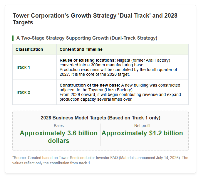
This disciplined investment plan, skillfully combining self-funded funds with government grants, is poised to capture the rapidly growing global customer demand in AI and data center sectors, solidifying its position as the overwhelming world leader in silicon photonics.
The semiconductor boom spreading from Hokuriku and its ripple effects on the regional economy
The total investment of 600 billion yen in Niigata and Toyama is expected to bring structural economic effects to the Hokuriku region, similar to what TSMC once brought to Kumamoto. Semiconductor manufacturing requires vast land, abundant clean water, and extremely stable power supply, making Myoko and Uozu ideal locations that combine these conditions. The impact is wide-ranging, from construction demand from new and expanded factories, to long-term job creation for high-tech professionals, logistics revitalization, and increased orders from local suppliers. Until now, Japan’s semiconductor strategy has tended to focus on Kyushu’s ‘Silicon Island’ and Hokkaido’s Rapidus, but with this decision, Japan’s semiconductor supply network will expand geographically. This initiative, which aligns local governments’ efforts to attract local governments and the Ministry of Economy, Trade and Industry’s subsidy scheme, will become a new model case for promoting regional revitalization from the perspective of economic security.
Future outlook and lessons to learn from “past failures”
The key to the success of this project lies in operating as planned, continuous production for ten years as a condition for subsidies, and adherence to priority supply to Japanese companies in emergencies. On the other hand, there are persistent concerns about past failures like Japan Display and Elpida Memory, where government-led interventions failed to translate into market competitiveness and ultimately prolonged the survival of “zombie companies” due to massive public funding. In this support for Tower Corporation, the focus is not on simply attracting a base, but on how to maintain profitability and technological superiority that allow us to continue winning in the global market. As subsidy wars unfold worldwide, for Japan to achieve a true ‘semiconductor revival,’ it is essential that public support goes beyond mere subsidies, but serves as a catalyst for autonomous private investment and continuous technological innovation.

コメント